

Representative Publications
1. M.D. BORYSIAK, K.S. BIELAWSKI, N.J. SNIADECKI, C.F. JENKEL, B.D. VOGT, AND J.D. POSNER. Simple Replica Micromolding of Biocompatible Styrenic Elastomers, in press Lab-on-a-Chip. 2013.
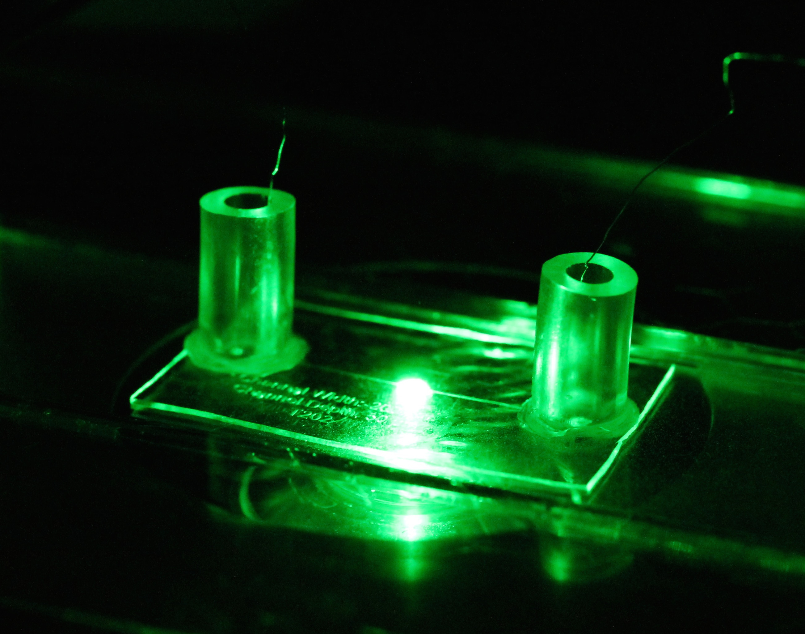
2. M.D. BORYSIAK, E. YUFEROVA, J.D. POSNER. Simple, low-cost SEBS microdevices for electrokinetic applications, Analytical Chemistry. 2013
Updated Device Fabrication
1. Create silicon wafer with SU-8 structures by standard photolithographic procedures.
2. Treat the wafer with silane treatment—e.g. trichloro(1H,1H,2H,2H-perfluorooctyl)silane—by putting the wafer in a dessicator with 50 µL of silane in a petri dish for at least 1 hour. Wash wafer with IPA and DI water following treatment.
3. Dissolve approximately 1 g of SEBS per 10 mL of toluene inside glass jar.
4. Mix thoroughly (at least 3-4 hours) on rotary mixer (or other mixing apparatus).
5. Sonicate mixture for 1-2 hours to ensure dissolution of polymer and to remove any large polymer globules. (Note this step can be skipped if the mixture is mixed well enough in step 2)
6. Place dissolved mixture in dessicator under low vacuum to ensure there are no trapped air bubbles. If significant bubbles are forming under vacuum, repeat steps 2 and/or 3 (generally air bubbles form when the polymer isn’t dissolved well enough). There should be no air bubble generation before proceeding to the next step.
7. Pour the de-gassed solution through a funnel onto the patterned wafer inside a PTFE coated ring (Norpro 666, from Amazon) and bake for 3h at 50-60°C and 10h at 85°C on a hotplate inside a fume hood.
7.1. Place a piece of foil with small holes over top of the solution to prevent wrinkles in the polymer due to fast evaporation of the toluene.
8. After evaporation is completed, heat the wafer to 40–45ºC on a hotplate to assist with de-molding. Gently remove the ring by scraping along with edges of the ring, both inside and out, with wafer tweezers or another flat tool. After removing the ring, gently peel the SEBS from the wafer.
9. Flat substrates can be made in the same manner as steps 2–8 with a non-molded silicon wafer with silane treatment.
10. Punch holes using a hand punch such as Fiskars 1/16” Circle Hand Punch (from Amazon).
11. To ensure good room temperature bonding strength, keep substrate surfaces as clean as possible. Handling inside of a laminar flow type hood is recommended for best bonding.
11.1. Heating devices under small pressure (e.g. small weight or paper clamp) to 80ºC in an oven for 30 minutes should improve bonding.